A new era for electronic materials
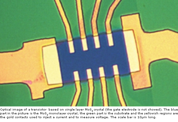
Impressive scientific developments are changing the way in which we look at electronic materials. For many different substances, it is now possible to realize perfect crystals only one or a few atom thick, whose electronic properties can be controlled in ways that would have been considered as science fiction only a few years ago. The latest discovery comes from the University of Geneva. A team of researchers succeeded in realizing transistors that turn a monolayer of MoS2 – an insulating material that does not spontaneously conduct electricity – into a material enabling current to flow without dissipating any power, i.e. a superconductor.

The possibility to produce materials of excellent quality having the thicknesses of a single atom has been demonstrated for the first time 10 years ago, through the discovery of graphene. Monolayer graphene is a one-atom-thick honeycomb lattice entirely made of carbon, whose extraordinary properties have impressive potential for future applications. It was initially considered to be unique, as other materials were not expected to preserve high-quality when thinned down to the atomic scale. As it turns out, this is not the case, and more compounds enabling the realization of high-quality atomically thin crystals have been discovered over the last few years, each with its own specific properties of interest. MoS2 – the material investigated by the scientists at the University of Geneva – is one of these.
In order to realize superconducting transistors, the Geneva team exfoliated macroscopic MoS2 crystal to extract individual monolayers, subsequently transferred onto a suitable substrate. Using state-of-the-art nano-fabrication techniques, they attached the electrical contacts necessary to inject current into the atomically thin crystal and to measure the resulting voltage. The devices comprise a gate electrode that – when energized by the application of a few Volts- enables the accumulation on the MoS2 monolayer of an electron density in excess of 1014 electrons/cm2. These very high values – a sizable fraction of an electron per atom present in the monolayer – can be reached thanks to recent technical developments, namely the use of an ionic liquid as dielectric layer separating the gate from the MoS2 monolayer.
At room temperature, the Geneva scientists found that individual monolayer MoS2 devices exhibit the expected transistor behavior. If no gate voltage is applied, MoS2 monolayers are insulating; upon energizing the gate, they start to conduct electricity. The discovery was made by cooling the devices down to low temperature in their conducting state. Below approximately 2 K, current was observed to flow at zero applied voltage, without energy dissipation. Experiments were performed not only on monolayers but also on bi, tri, and thicker layers, all of which are intrinsically insulating when no gate voltage is applied. In all cases superconductivity could be induced by using the gate electrode to accumulate electrons.
These results represent the first observation of superconductivity in a crystal after reducing its thickness to the ultimate atomic limit. Besides its scientific relevance, this discovery showcases how electronic materials are entering a new era. It is now not only possible to produce structurally perfect monolayers of different substances, but also to manipulate them, to control their electronic behavior, and to combine them together to create artificial systems with new properties. Even for the experts in the field, these developments are mesmerizing, and would have never been foreseen only a short while ago.
Although progress is fast, much research is needed to understand the quantum mechanical laws that govern the electronic properties of these new atomically thin materials. This is not science fiction any more: it is the forefront of science. It will not happen tomorrow, but there seems to be little doubt, that in the longer term the development of materials engineered at the atomic scale will seriously impact technology.
The research team, composed by Davide Costanzo, Sanghyun Jo and Alberto Morpurgo, is part of the Departement of Quantum Matter Physics and of the Group of Applied Physics at the University of Geneva. The work, which relied on crystals provided by Helmuth Berger at EPFL, is supported from the Swiss National Science Foundation and the project of the European Community “Graphene Flagship”. Several research groups at the University of Geneva, as well as at different Universities in Switzerland, are investigating the the atomic scale electronic properties of new quantum materials – including crystals with thickness of only one or few atoms- and have international leading roles in this field of research.
Contact :
For more information, please contact Prof. Alberto Morpurgo (Tel. +41 22 379 35 74).
January 15, 20162016
